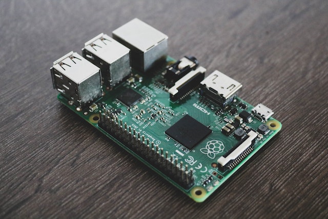
A printed circuit board (PCB) is a flat, rigid sheet of non-conductive material that has electrical connections etched or printed into it. It is used to build and interconnect electronic components in order to create functional circuits. PCBs are commonly found in all types of electronics, from mobile phones and computers to home appliances and industrial machinery.
Different Types of PCBs
There are four different types of printed circuit boards: single-sided, double-sided, multi-layered, and flexible. Single-sided PCBs contain a single layer of copper traces on the surface. Double-sided PCBs have two layers of copper traces on each side with a thin non-conductive layer in between. Multi-layered PCBs contain multiple layers of copper traces on each side, separated by insulating materials. Finally, flexible PCBs are made from flexible materials such as plastic or Kapton and can be used for applications where flexibility is required.
Components of a PCB
A. Copper Layers
The copper layers are the most important component of a printed circuit board (PCB). The copper layer is etched with electrical connections that create the desired circuit. This task can be completed manually or through the use of an advanced computer-aided design program.
B. Solder Masks and Silkscreens
Solder masks and silkscreens are applied to the surface of the PCB after the copper layers have been etched. The solder mask is usually a thin layer of plastic that helps to prevent solder from bridging between connections and thus causing a short circuit. The silkscreen is printed with the component identification information and helps to make it easier to assemble the PCB.
C. Through-Hole Components
Through-hole components are components that are soldered directly into the holes of a PCB. These are usually used for larger components such as capacitors, resistors, and transistors. Through-hole components are sometimes referred to as “plated-through hole” components because the pins are plated with solder prior to soldering.
D. Surface Mount Components
Surface mount components are components that are soldered directly to the surface of a PCB. These are usually used for smaller components such as integrated circuits (ICs) and light-emitting diodes (LEDs). Surface mount components are sometimes referred to as "surface mount technology" (SMT) components because they are soldered directly onto the PCB without the use of through-hole techniques.
Process of Manufacturing PCBs
Step 1: Designing the PCB
The first step in the PCB manufacturing process is to design the PCB. This includes creating a schematic diagram of the circuit, choosing components, and laying out the copper traces on the board. Whether you prefer to create your design by hand or with the assistance of a computer-aided design (CAD) program, both methods will give you the desired result. With the design finalized, it's time to put the plan into action and send it off for production.
Step 2: Creating the Master Artwork
Once the PCB design is complete, the manufacturer will create a master artwork from the schematic. This artwork is used to transfer the desired circuit onto the board. The artwork may be printed or etched using various techniques such as silk screening or photolithography.
Step 3: Printing the Layers onto Copper Laminate
The next step in the PCB manufacturing process is to print or etch the desired circuit onto a copper laminate. This layer will become the base for all other layers of the board and provides an electrical connection between components. The printed or etched layer can be either single-sided, double-sided, or multi-layered depending on the complexity of the design.
Step 4: Drilling the Holes
The next step in the process is to drill the holes for components and pins. This is done using a CNC machine or a manual drill press, depending on the size and complexity of the board. The holes need to be precisely drilled to ensure proper fitment of components and pins.
Step 5: Adding Solder Mask and Silkscreen Layer
The next step is to add a solder mask and silkscreen layer to the board. The solder mask helps to prevent short circuits by preventing the solder from bridging between connections. The silkscreen has component identification information that makes it easier for assembly workers to place components correctly.
Step 6: Adding Electrical Components
The next step is to add electrical components such as integrated circuits, capacitors, resistors, and other parts. Depending on the type of component, it can be soldered either by hand or with a reflow oven. After assembling all the necessary elements, it's time to evaluate how effectively this board operates.
Step 7: Testing the PCB Assembly
The last step in the PCB manufacturing process is to test the board for functionality. This can be done manually or with an automated tester that verifies each component and ensures proper electrical connections. Once the board has passed all tests, it is ready for use.
Benefits of Using PCBs in Electronics Manufacturing
Reduced Size of Electronic Devices
One of the most obvious benefits of using PCBs in electronics manufacturing is that they can reduce the size of electronic devices. By eliminating wires and other components, PCBs allow for more compact designs with fewer parts. This makes it easier to fit complex circuits into small spaces, such as mobile phones and watches.
Improved Efficiency and Performance
Using PCBs can also improve the efficiency and performance of electronic devices. By providing a reliable electrical connection between components, PCBs reduce the risk of shorts and other problems caused by loose wires. This allows for data transfer rates and better overall performance in electronic devices.
Reduced Costs and Time to Market
Lastly, using PCBs in electronics manufacturing can also reduce costs and time to market. By eliminating the need for complex wiring or manual assembly, PCBs can significantly reduce production costs and speed up the process of getting products to market. This can be especially beneficial for startups who are looking to launch their products quickly and cost-effectively.
Conclusion
PCBs are an essential part of electronics manufacturing. They provide a reliable electrical connection between components, reduce the size and complexity of electronic devices, improve efficiency and performance, and can help to reduce costs and time to market. By understanding the PCB manufacturing process and its benefits, you can ensure that your product is designed for maximum reliability and performance. One of the best manufacturers of PCBs is Pad PCB. They use a variety of production processes to create custom PCB designs for various applications.
Add new comment